PCB Terminology / Glossary - Blind Via
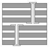
Via: A plated through hole (PTH) in a Printed Circuit Board (PCB) that is used to provide electrical connection between a trace on one layer of the Printed Circuit Board to a trace on another layer. Since it is not used to mount component leads, it is generally a small hole and pad diameter.
Blind via: A via hole that does not pass completely through the printed circuit board. A blind via starts from one side or another.